Trending Topics

 Trending
Inside Intel’s Fab 52 and the Intel 18A process

“No cameras. No smart glasses. No smartwatches. Nothing smart at all.” These were the words greeting a hotchpotch of European journalists as we climbed out of our air-conditioned coach and into the warm, humid embrace of Arizona in late September. Brits, Germans and French alike murmured their assent as we stepped onto Intel’s Ocotillo campus, home of Fab 52.
This is the fifth Fab that Intel has built on the site, and only its second to churn out chips based on the Intel 18A process.
Now, 18A is both tiny – 1.8 nanometres, which the 18 refers to, is about the same size as seven silicon atoms placed side by side – and huge. It would be hyperbolic to say that Intel’s future rests on the success of this one manufacturing process, but its reputation as a global force in chipmaking has been hurt this past decade. It needs a hit.

Why Intel 18A matters
Intel 18A is such a big deal for three reasons (and more, but I’ll stick to three). First, it’s the foundation on which Intel’s next-generation mobile chips, codenamed Panther Lake, will be built. Likewise Clearwater Forest, now officially launched as Xeon 6+.
Second, this will be the process on which future processors are based. It’s a chance for technologies such as RibbonFET and PowerVia to shine: together, these improve performance per watt and chip density. If Intel gets 18A right, and that means delivering at scale, then it’s set fair for the next 2-5 years (at which point its attention will switch to the already announced Intel 14A, based on a 1.4 nanometer process).
The third reason: because it puts Intel, and the USA, back on the map when it comes to foundries. It could halt a 25-year slide that has seen Intel move from global player to bit player, with its once great rival TSMC now dominating the foundry market with a 65% market share according to recent reports.
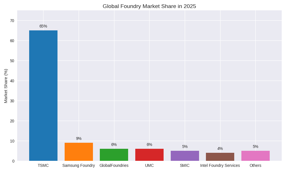
Indeed, if Intel can get its yield right then we might even see AMD build chips based on its technology. Not to mention Nvidia, now a 4% shareholder in Intel, although it has yet to commit to using Intel Foundry Services.
Inside Intel’s Fab 52
The key part of any Fab tour is to get into your “bunny suit”. The suit’s aim is to capture any motes of dust, hair or fabric that might escape, with only the upper half of your face open to the air. Gauze masks cover hair and beards, despite being fully enclosed by the headwear, with any gaps sealed and double-sealed.
Security was just as tight. Forget trying to smuggle in your phone; even if you did there was nowhere to put it (although one of our number reckoned he could have snuck in with smart glasses).
So there we were. Having been divided into groups of six to eight people, we intrepid explorers were about to set forth into a factory that’s cleaner than an operating theatre. Much cleaner in fact: unless I misheard our guide, Fab 52 meets ISO 2 standards, which means up to 100 particles per cubic metre. Most operating theatres are closer to a million particles.
Step into the light

I’d like to add drama here. That the whole process was like stepping into the future. That we had to pass through a separate portal were mini robots scanned our bodies for errant particles. But no. We walked through a door and into the Fab.
To be precise, into Fab 42, which came online in 2017 and makes many of the Intel chips already has on sale. The most exciting feature were the FOUPs, whizzing away on rails above us. FOUP stands for “front opening unified pods”, and is a sign that Intel’s geeks need to work on their acronyms. Surely a Star Wars-inspired name could have worked – Relaying 2D Discs Too? Carrying 3D Packages Overhead? – but no.
Perhaps they were more concerned that these robots simply worked as effectively as possible, with their job being to take the wafers from one machine to the next.
Intel sent me two separate written messages saying that I couldn’t name any machines, on top of all the verbal warnings during the tour, but it’s public knowledge that it uses EUV lithography scanners made by ASML.
While machines do all the manufacturing work, we walked past numerous bunny-suited engineers as we walked through Fab 42. They’re essential to keep the machines running, which they have to do 24/7. Once a Fab is open, it doesn’t stop until it’s time to be decommissioned. It just wouldn’t make financial sense, such is the financial investment in each Fab – think roughly $25 to $30 billion.
Now step into Fab 52 – and the yellow light

Walking through Fab 42 took around five minutes, if you include pit stops where our guide explained what we were looking at. Well, very vaguely. He named no names, and he was as willing to answer questions about the machines as a teenager is their love life. The best way to avoid journalistic traps is to say nothing, after all.
Then we all saw the light. We moved from the bright, almost antiseptic conditions of Fab 42 to the yellow-bathed Fab 52. This is necessary to filter out wavelengths of light that might affect the chemicals used to create patterns on the wafers. You can still see clearly, but I couldn’t imagine working in those conditions all day. Or all night.
For a moment I thought I was imagining things when I saw an engineer approaching in an orange suit, but our guide was authorised to tell us that this showed people who worked with potentially hazardous materials (including copper, unless I misheard). So no fist bumping in the corridors.
And that was it. Having walked less than 200 feet into Fab 52, our tour came to an abrupt halt. Perhaps because of time limits, perhaps because Intel didn’t want us to see the far end of the halls where the Oompa-Loompas live.
Back onto safe ground

code-named Panther Lake, outside the Intel Ocotillo campus in Chandler, Arizona
It turned out to be a shorter tour of the Fabs than I expected, but that’s okay. The really interesting stuff happens inside the machines, after all. Plus bunny suits don’t become more pleasant to wear over time, and there’s a lot of noise – much of it coming from the vents that continually draw HEPA-filtered air down from the top and into grates in the floor. This ensures any particles that do escape head downwards as soon as possible.
None of this can describe the scope of what Intel has built, however. Before the tour, Intel drove us around its campus, which took 18 minutes on a coach. Much of that was past swathes of land that could be used to build yet
more Fabs, of the huge water processing plants Intel uses to ensure that it’s “water positive”, of the immense car parks for the tens of thousands of Intel employees and contractors. Little wonder that this Fab is effectively built in the middle of a desert: you need the space.
There are unanswered questions from the tour, far beyond the ones that our guide refused to engage with. Will Intel hit the yields it needs to make 18A a success? Will its strategy of opening up its foundry business to others prove the right long-term move? Come 2029 and the departure of Donald Trump from the Oval Office, will the next President back USA-based manufacturing with the same passion? And the same financial packages?
Perhaps by then it will be moot. If Intel Foundry Services can deliver at scale then the cash will follow and handouts from the US Government will be long-distant history.
Related articles
- What is Intel Xeon 6+ in Intel’s own words
- Exclusive interview with Kira Boyko, Product Line Director, on Intel Clearwater Forest: “You’re going to see a 750 kilowatt reduction and then 3.5x performance”
- Intel uses Computex 2025 to announce workstation-class GPUs plus Gaudi 3 and AI Assistant Builder availability
About The Author

Tim Danton
NEXT UP